I’m currently in the process of building a computer based on the 6502 microprocesser, following Ben Eater’s instructions. It’s a nice way of learning the lower level parts of a computer by wiring up and eventually coding everything yourself.
In this post I want to share my (more or less structured) notes of the steps taken and lessons learned so far (covering part 1 to part 7). While my notes were mainly created to explain things to myself, I hope you can get some value out of it as well.
If you’re interested in building the computer yourself, follow along Ben’s videos and consider buying the parts directly from him to support the content.
Part 1
Video: “Hello, world” from scratch on a 6502
Notes and steps taken:
- The 6502 is an 8-bit microprocessor introduced in the 70s and was used in popular home computers (like the Apple II or C64) in the 80s
- A more modern version, the W65C02, is available since the 80s. The W65C02’s static design allows us to stop the clock while preserving the contents of the registers (which is not the case with the older design).
- Getting an overview of available input and output pins; we have 16 bit addresses and an 8 bit data bus
- Connect the clock (phase input) – I highly recommend building the system clock yourself as well (Astable 555 timer - 8-bit computer clock) such that you are able to single-step through instructions manually (which helps with understanding and is great for debugging). You can later swap it with a crystal oscillator.
- Add a reset button to be able to reset the processor (using the RESB pin which must be held low for at least two clock cycles to reset/re-initialze)
- Use an Arduino Mega to capture the states of the address pins and the data bus to get an understanding of what the microprocessor is doing
- The connected pins are set to INPUT (
pinMode) on the Arduino and then read in the loop (digitalRead). The bit values are printed to the serial monitor (in the Arduino IDE). - As we want to see the state after each clock pulse, we connect the clock to the Arduino as well. We then attach an interupt for the clock signal,
attachInterrupt(digitalPinToInterrupt(CLOCK), onClock, RISING);, whereCLOCKis pin 2 on the Arduino andonClockis the function containing thedigitalReads. This allows us to read the state of the address and data lines (and whether the data bus is currentlyreadorwrite, i.e. if the processor is currently reading from or writing to the data bus) whenever we get a pulse from the clock (instead of continously in the main loop). - The Arduino program will actually be pretty helpful later on during debugging. One tip I can give you is to leave some space on the address and data bus lines on the breadboard. It can get pretty tight there and you don’t want your debugging tools to be hard to use every time you have a problem.
- With the Arduino monitoring the address and data lines, continue to hard-wire a value (i.e. just connect some resistors to ground or 5 volt for a 0 or 1, respectively) on the data bus. The value we hard-wire is 11101010, or 0xEA, which is the NOP instruction for the 6502 processor.
- Having a sensible input on the data bus (even if it doesn’t do anything) lets us see much more clearly what the processor is doing: going through its 7-step intialization process as described in the data sheet when pressing the reset button, and then loading the start address of the program from address
0xfffc(low byte) and0xfffd(high byte). In our harcoded case the address comes out as0xeaea. And when the processor sets its address pins to the start address of0xeaeaand reads again from the data bus, it gets0xeaagain (as that’s still the hard-wired value on the data bus) but this time treating it as an opcode for no instruction (NOP =0xea, see datasheet). The processor then continues incrementing the address (to0xeaeb,0xeaeb,...) every second pulse (as NOP takes two clock cycles) and reading another NOP. This goes on forever.
Part 2
Video: How do CPUs read machine code?
Notes and steps taken:
- Install a 28C256 EEPROM (electrically erasable programmable read-only memory) which can store 32 kilobytes (or 256k bits) of data
- Most of the pins are for addressing and I/O. We can set the address pins to a particular location to read the data (via the I/O pins) at that location on the ROM chip (which is what the processor will do). All address lines and data bus lines of the microprocessor would be connected to the address and I/O lines of the EEPROM.
- Problem: the 6502 has 16 address pins (A0 to A15), the EEPROM only 15 (A0 - 14). So while the processor can access 65,536 (16^2) locations, the EEPROM only has 15 address pins as it can only store 32,768 bytes (2^15) of data. If the processor would sets its address pins to a value greater
0x7fff(32,767) it would start reading the contents from the beginning of the ROM again (as A15 of the microprocessor would be set high but only the pins of A0 to A14 would be connected to the ROM,1000 0000 0000 0000to000 0000 0000 0000). - Possible solution: connect A15 to “Chip Enable” (CE, active low) pin of EEPROM so it would only output data when CE is low. Once the microprocessor would try to access higher addresses, the ROM wouldn’t output anything, meaning we could use the upper address space for something else.
- Still a problem: as descibed in part 1, the processor wants to read the program start address from
0xfffcand0xfffd(which is greater than0x7fff) after its initialization. - Solution: invert signal from A15 to set CE to low when the top bit is set, and high when it is not. This way we have mapped the lower addresses to the higher addresses and can use the lower addresses of the microprocessor for something else.
- Wiring: connect the address (A0 to A14) and data bus pins from the 6502 to the address and I/O pins of the EEPROM. Set further control pins as instructed. Connect A15 of 6502 to inverter (NAND gate) and output of the inverter to CE.
- Create a file with 32k NOPs (
0xea) and write it onto the ROM (to reproduce the behavior of the hard-wired NOPs from earlier). Remember for later that data at location0x0000in the file will get accessed when the microprocessor asks for data at0x8000, since we hardwired this offset via the A15 -> inverter -> CE above. So we’ll always have this 32,768 byte offset for the ROM locations. - Now change the file of NOPs at location
0x7ffcand0x7ffd(instead of0xfffcand0xfffd, remember the offset!) to set the start address to the beginning of the ROM, which is accessed as0x8000by the microprocessor (but is actually0x0000in the ROM). Confirm with the Arduino that reading the data from0xfffcand0xfffdafter the initialization steps in fact returns0x8000(or rather0x000x80, as it’s stored in little endian). - Create a more interesting program and store it at the beginning of the ROM (
0x0000, or0x8000to the microprocessor):A9 42 8D 00 600xa9is the opcode for load A (lda) with an immediate value (the 8-bit A register is the main register on the 6502)0x42is the (arbitrary) value we want to load into the A register0x8dis the opcode for storing the contents of the A register to an address (sta)0x6000would be the target address where the contents should be stored
- Running the program we see (monitoring with the Arduino) that the instructions are executed as expected and that the processor eventually wants to write the value
0x42to address0x6000(address pins =0x6000, data bus =0x42). But, of course, we don’t have any memory (or other hardware) connected yet :-) - We need to find a way to have external hardware respond to certain addresses such that, for example, the
0x42on the data bus from above could be stored somewhere. We’re going to use the W65C22 VIA (Versatile Interface Adapter). - The W65C22 is made to work alongside the 6502 microprocessor. Essentially, it has D0 to D7 pins that we can connect to our data bus, PHI2 to connect our clock signal to, RW to be in sync with the read/write of the 6502 and chip select pins to indicate when the 6502 is talking to the 65C22. The Port A and Port B pins of the 65C22 can be used for I/O. For example, we can latch data from the data pins to eventually send it to some other device (capture the data lines during a write, and then hold the value until we need it, while the processor can already continue doing other things). We also wire up the reset pin (RESB, active low) to our existing reset button.
- How can we implement the address decode logic to know when the W65C22 needs to be active? We want the 2 CS (chip select) pins to be active (high and low) when the microprocessor has
0x6000(0110 0000 0000 0000) on its address pins. The first two bits can go through NAND gates to output 0 when they are matching 0 (A15) and 1 (A14). This 0 can go directly to the CS2 which is an active low. A13 can be connected directly to CS1 as it’s an active high. With this setup the W65C22 will be enabled from0x6000(0110 0000 0000 0000) to0x7fff(0111 1111 1111 1111) (as we don’t specifically handle the bits below A13). - Now we just need to wire up the register select pins, so that we can output from a register through the port A and port B pins (or use other functions). We will use the lower bits of the address (A0 to A3) to control this register selection.
- Verify the wiring with a program that outputs to port B:
A9 FF 8D 02 60 A9 55 8D 00 60 A9 AA 8D 00 60 4C 05 80 ... 00 80 ...- load
0xffinto the A register of the 6502 (0xffsuch that we set all the bits (1111 1111) of the data direction register on the 65C22 to output, 1 meaning “output”, see datasheet) - store the contents of the A register to address
0x6002(addressing data direction register B which is register 2, addressed as0x6002as A0 to A3 have to be0010) - now that we’ve set all pins of port B to output, we can store the value we want to latch, targeting register 0 (register “B”) at
0x6000. We are writing0x55to just light up every other LED connected to port B (as0x55is 0101 0101). The instruction is:A9 55 8D 00 60(lda #$55,sta $6000) - to make the LEDs blink, we can next flip the bits of
0x55(0101 0101), writing0xaa(1010 1010) usinglda(0xa9) andsta(0x8d) again - and then create an inifite loop by jumping back to the instruction of loading
0x55(which was at location0x8005):4C 05 80(0x4cbeing the opcode forJMP) - we keep the start address at
0x8000(0x0000in the ROM) as we start reading the program from the beginning of the ROM
- load
Part 3
Video: Assembly language vs. machine code
Notes and steps taken:
- Write the previous program in assembly and use the vasm assembler to convert it back to machine code
- Some hint regarding structuring the assembly code:
- Use
.orgdirective to indicate to the assembler at which location the program is to be expected in memory. So.org $8000would indicate that the instruction after this directive is to be found at address0x8000(which of course is actually0x0000in the ROM). In the same way we can use.org $fffcto set the start address of the program. Writing.word $8000after this.orgdirective would thus be equivalent to setting the values00 80to0x7ffcand0x7ffdin the ROM file. Remember that without the.org $8000directive, the assembler wouldn’t know that our program on the ROM maps to0x8000to the microprocessor and would expect it to start at0x0000. This in turn would let the assembler write the start address to0xfffcinstead of0x7ffcleading to a rom file twice the size (from0x0000to0xffff, so 65,536 instead of 32,768 bytes).
- Use
- Improve program to use labels, then change it to output a different LED pattern: start with
0x50(0101 0000), thenror(rotate right) to let the active LEDs move to the right.
Part 4
Video: Connecting an LCD to our computer
Notes and steps taken:
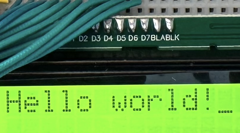
- Connect HD44780 LCD display to breadboard; add a variable resistor to be able to adjust brightness, connect port B lines from W65C22 to the data lines (D0 to D7) of the display; connect the three top bit pins from port A of the W65C22 to the control pins RS (register select), RW (read/write) and E (enable) of the display.
- The data lines of the display are able to access a data register (DR) or an instruction register (IR) – which register is actually accessed/written to is determined by the control signals that we connected to port A of the W65C22. RS (register select) high means we are targeting the data register, RS low means we are targeting the instruction register (for controlling the behavior of the display). The actual reads or writes are happening once the E (enable) pin is set high.
- Improve previous assembly program to set some constants for port A and B (
PORTA,PORTB) and the data direction registers A and B (DDRA,DDRB) - In addition to setting all pins of port B to output, we do the same for the connected top three bits of port A (
lda #%11100000,sta DDRA) - With the port A (top 3) and B (all) pins connected, we can send instructions to the display. Going through the example:
- Set data length, number of lines and character size with RS = 0 (we want to send an instruction), R/W = 0 (we want to write), D5 = 1 (function set instruction), D4 = 1 (data length 8 bits), D3 = 1 (2 line display), D2 = 0 (5x8 dots per character), D1 and D2 aren’t relevant (see instructions in table 6 and table 13 in data sheet). Encoding this in our assembly program would be:
lda #%00111000,sta PORTB(load the values for the data lines into the A register of the 6502, store contents of A register to address of register B/port B on W65C22). Then clear the control signals on port A:lda #0,sta PORTA. And then set the enable bit (E) to actually send the instructions to the display’s registers:lda #E,sta PORTA(whereE = %10000000) and immediately afterwards clear the control signals again. - Continue in the same fashion for sending instructions for display on, entry mode (we want the address counter to increment with each character sent to have our text written left to right) and eventually to write a character.
- To write characters we need to set the register select (RS) to high to target the data register of the display and then put the ascii value of the character on the data lines and write it by toggling the enable bit
- Test out the program by writing it to the ROM, powering on the circuit and holding reset. We see the letters appear on the screen.
- Set data length, number of lines and character size with RS = 0 (we want to send an instruction), R/W = 0 (we want to write), D5 = 1 (function set instruction), D4 = 1 (data length 8 bits), D3 = 1 (2 line display), D2 = 0 (5x8 dots per character), D1 and D2 aren’t relevant (see instructions in table 6 and table 13 in data sheet). Encoding this in our assembly program would be:
Part 5
Video: What is a stack and how does it work?
Notes and steps taken:
- Improve “Hello World!” program by creating subroutines for
lcd_instructionandprint_charand then jumping there withjsr, and returning withrts. - Try the program again by writing it to the ROM. It doesn’t work anymore since we now use subroutines but don’t have a stack where to store the return addresses. So while the microprocessor tries to store the return address before jumping to the subroutine, there’s no hardware (RAM) available to actually store that address. And then, when
rtsis called, there’s no way to retrieve the return address. - The 6502 expects the stack to be in the memory area
0x0100to0x01ffand has an 8-bit stack pointer (0x00to0xff, 256 bytes). - We can use
txsto transfer a value from register X to the stack pointer (ldx #$ff,txs) if we want to initialize the stack pointer in the beginning (the stack grows downwards towards the lower addresses, just like on other platforms).
Part 6
Video: RAM and bus timing
Notes and steps taken:
- Install 62256 RAM chip (256k bits, 32 kilobytes)
- The pinout is the same as for the ROM chip, so we can just wire the address and data lines from the ROM chip to the address and data lines of the RAM chip. And the WE of the RAM can be connected to the RW pin of the 6502.
- The planned address layout will be:
0x0000to0x3fffreserved for RAM (0x0100to0x1ffffor stack),0x8000to0xfffffor ROM (as before). We cannot just give the RAM the whole upper part of the 65,535 addresses as we still have to address the interface adapter (see above). - While the RAM wouldn’t need all that space, it’s easier to build it this way; we just need to check that A15 and A14 are low to detect if we’re addressing the RAM (as this covers the addresses
0x000to0x3fff(0011 1111 1111 1111)). - We could wire up A14 and A15 of the microprocessor to OE (output enable, active low) and CS (chip select, active low) of the RAM as this would cause the RAM to only be active and output data whenever we’re in the above mentioned address range (with A14 high and A15 low we might still write to an area we’re not using, but it wouldn’t cause problems as we would never output that data). However, we haven’t yet looked at the timing of the microprocessor and RAM and if they would actually be compatible in our setup (as it takes some time to set up the address lines and control signals, and for the RAM to output valid data after it is addressed).
- Analyse read timing waveform of the RAM and compare to timing diagram of 6502
- We’re planning to run the processor at a maximum of 1 MHz and will calculate the timing based on that. So when looking at the timing diagrams mentioning nanosecond durations, we will assume that we have at least 1,000 nanoseconds in one clock-cycle.
- It can take up to 70 nanoseconds for the RAM to output valid data after the addresses and control signals are set up correctly, so the microprocessor needs to wait at least this amount of time before (or continue) reading the data after setting the address. There’s also an additional timing requirement by the microprocessor where the data must be held valid. Both are confirmed to be OK after analysing both datasheets.
- Trying to confirm the write sequence as well. We see that we need to make sure that CS (connected to A15 in our circuit) needs to go high before any of the other address bits change (same with RW<->WE). We cannot expect this to be true based on the information in the datasheet. And the same is true for the timing when CS and/or WE go low before the beginning of a write.
- Can we slightly delay setting the CS to low after the address becomes valid and setting it to high before the address and data become invalid again? It turns out we can just tie it to the clock (phi2) because the clock rising falls into the range where the address is already valid and falls low before the address becomes invalid and RW goes high.
- With two logic gates we can make sure CS goes low only when the clock is high. We can connect A15 through a NAND gate to invert it (low becomes high) and connect this output together with the clock signal as inputs to another NAND gate, thus outputting a low only when the clock is high and A15 is low (i.e. high output of the first “inverter” NAND gate). The timing of the NAND gates themselves is short enough that it does not affect our circuit.
Part 7
Video: Subroutine calls, now with RAM
Notes and steps taken:
- Wire up A14 to OE, and A15 through the NAND gates to CS as described above
- Tie inputs to 4th NAND gate to high; just for good measure
- Improve “Hello World” program to clear screen when setting up the display in the beginning (
#%00000001)
✉️ Have a comment? Please send me an email.